8-bit CPU: Memory
Time for another important part of the computer - memory. Here I think I have to come up with my own design. Ben's version has only 16 bytes, uses nowadays-exotic 74189 memory chips and there are DIP switches for programming.
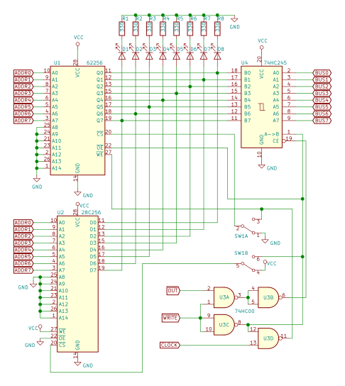
For the memory I plan to use 62256 SRAM chip. It can store 32 KiB of data, I initially plan to use just 256 bytes, so I'll connect remaining address pins to GND.
I'm also not in a mood for any DIP switch based programming, so I'll add an EEPROM instead. There are several ways how computer can utilize such setup:
- split the address space into program and data memory. This is how Ben's 6502 breadboard computer works. Some additional logic gates are used for chip selection, the main issue however is that it is not very flexible.
- use Harvard architecture, where program and data memories are completely separate. Reading and fetching instruction are two different operations: former accesses RAM, latter - ROM. This is how AVR microcontrollers (heart of Arduino) works. It would give total amount of 512 bytes. The downside, however, is that one can not run programs from RAM. No live-patching, new versions of program always require re-flashing the EEPROM.
- copy contents from ROM into RAM on startup. There are several ways how to do it. James Sharman built dedicated hardware for it. My plan is to provide a special bootloader mode, where all reads comes from ROM and all writes goes into RAM. Then I'll add bootloader code at the beginning of programs (it should take just a few instructions) that copies everything into RAM.
Small challenge was that in 62256 RAM data pins are used for both input and output, while 74189 has a set of separate input and output pins. Turned out, this works very well with 74HC245 buffer chip's bidirectional feature.
Internally there are 4 control lines: OE and WE for RAM chip, DIR and OE for buffer chip. I, however, wanted to provide a bit higher-level control. Also, writes should occur only on clock.
Direction control was easiest: when RAM's output is enabled, buffer chip should be in "to Bus" mode. When RAM is about to be written, OE is disabled and buffer should be switched in "from Bus" mode.
After playing around with Logisim simulations I came up with following "formulas":
- RAM_OE = not(WRITE)
- BUFFER_DIR = RAM_OE
- RAM_WE = CLOCK nand RAM_OE
- BUFFER_OE = not(OUT nand WRITE)
Note that there is no edge-detection of any kind for the clock signal. That's because I have another idea how to handle it - in Clock module.
How does ROM and bootloader mode come in? In normal mode, RAM's CE pin is always Low (enabled), while ROM's - always High (disabled). In bootloader mode RAM's CE is connected to WE, so RAM is enabled only when writing to it. At the same time ROM's CE is connected to RAM_OE, enabling it for reads. In schematics mode switch is handled by SW1.
Enough with the theory, let's build it already! I started by soldering up two more Register boards. Why? First, I need a register for MAR. Whole thing will not fit on single breadboard, but only couple of chips goes to second one, so there's space for another board. Let's say - that could be an Instruction Register, I won't use it right now, but it will be wired and ready to go, when I'll need it.
In theory both MAR and IR does not need all output features, so I could leave out few chips, but I plan to later reuse them as general purpose registers C and D, so I still did a full build.


Comments
Post a Comment